European Packaging, Assembly, and Test – Workshop 2023
Aiming at facilitating mutual engagement, the European Packaging, Assembly, and Test – Workshop 2023 will foster collaboration among semiconductor packaging, assembly, test manufacturing, and design experts along the complete semiconductor packaging supply chain, to collectively strengthen the semiconductor packaging eco-system in Europe.
Key topics presented
- European market and supply chain
- European OSAT industry capabilities
- Device and packaging manufacturers trends in challenging times
- Advocacy for the packaging, assembly, and test industry in Europe
- Reliability and quality of electronic devices and systems
Highlights
- Exciting Exhibition
- Seminal Keynotes
- Invited Speakers
- Official visit to Sencio Facility
- Networking and business opportunities
- Social evening event
Registration
EuroPAT Workshop 2023 |
|
Early Bird, 15.05. – 15.07.2023 280,00 € incl. 21% VAT 350,00 € (incl. 21% VAT) from 16.07.2023 |
|
| Register now |
ESiPAT-TC members are entitled to a discounted rate. During the early bird phase (until 15 July 2023), the workshop ticket for ESiPAT-TC members costs 250 € including 21% VAT. From 16 July 2023, the price will be 320 € including 21% VAT.
Venue
Noviotech Campus
Transistorweg 5, Building M,
Nijmegen,
Gelderland 6534 AT,
The Netherlands
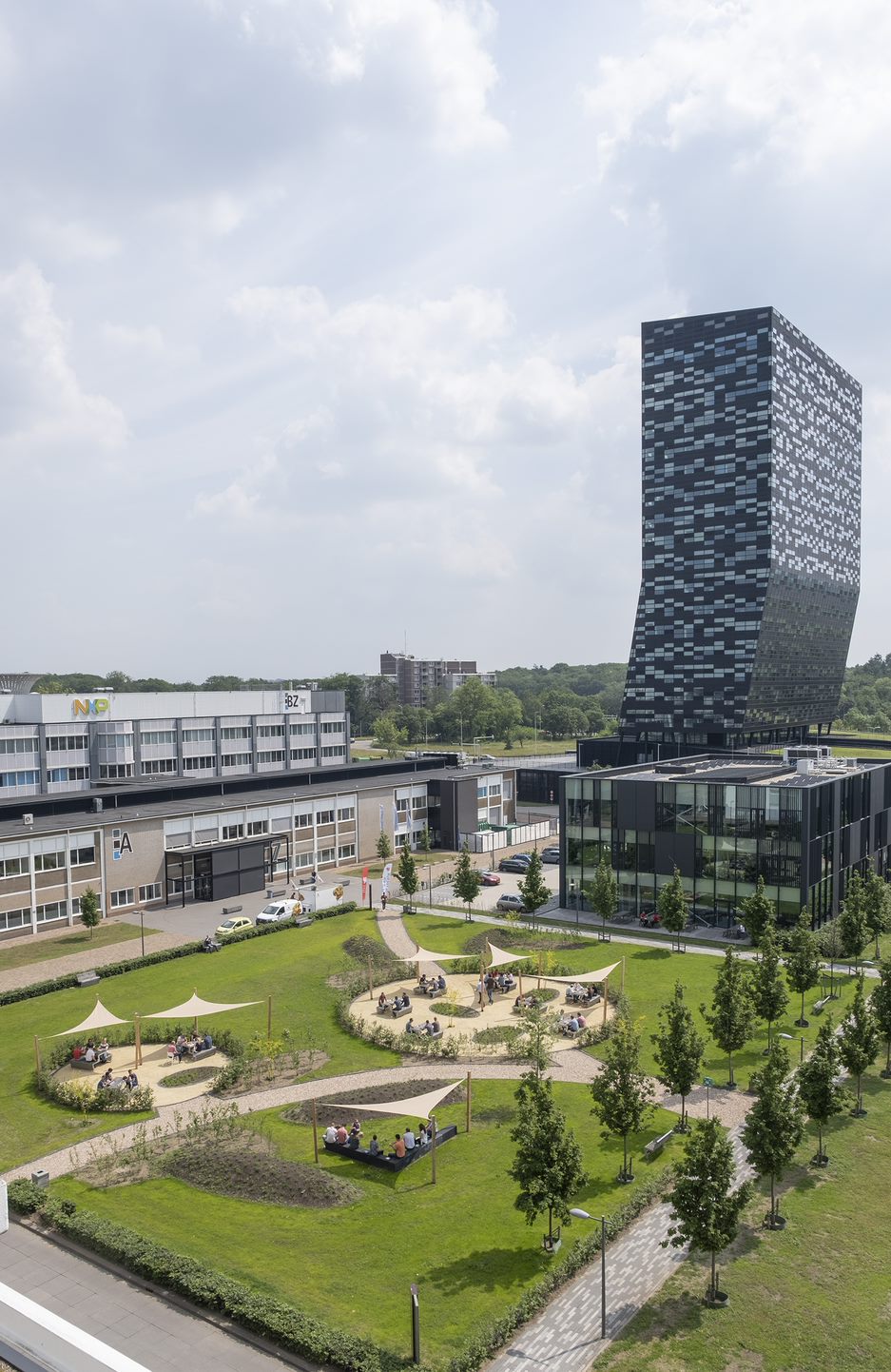
Noviotech Campus aims to become the city campus of the future. A green, lively, healthy and safe environment, the place to be for innovators in Health & High Tech. With architectural powerhouse MVRDV – and supported by our partners in the region – we captured our vision into the masterplan 2022 – 2027.
Accommodation

Hotel Nimma
Weurtseweg 478
6541 BE Nijmegen
Online booking and pay online or leave a credit card reservation.
If you want to make a reservation with us, you can do by our own website www.hotelnimma.nl or by www.booking.com
Our own website is slightly cheaper than www.booking.com.
welcome@hotelnimma.nl
restaurant@hotelnimma.nl
www.hotelnimma.nl
+31 (0) 24 8444007

Sanadome Hotel & Spa Nijmegen
Sanadome Hotel & Spa Nijmegen | Weg door Jonkerbos 90, 6532 SZ Nijmegen | 024 – 359 72 18 | Sanadome.nl
The guests can book via our website and use the code NTC06092023 for the discount. Below, you can find a picture of the website, as you can see, it is possible to enter the code (promotional code).

Please note, the discount is only available for 50 hotel rooms and the code is not useable any longer when this amount is reached.

Hotel Nijmegen-Lent
Hertog Eduardplein 4 | Nijmegen-Lent
| Discount | 10 % on the best available refundable roomrate per night |
| Applicable to | Queen-, Comfort Corner- and Comfort hotelroom |
| Code validation period | From 17 March 2023 until 29 August 2023 |
| Maximum number of rooms per night* | 25 |
| Applicable booking period | From 5 September 2023 until 6 September 2023 |
| Payment | Guests own expenses |
| Cancellation policy 1-7 hotel rooms |
The room can be cancelled free of charge up to 12:00 noon on the day of arrival. If the room is cancelled after this time or in case of a no-show, 100% of the reservation value of the first night will be charged. If the reservation consists of multiple nights only the first night will be charged and the remaining nights will be cancelled. |
| Booking options | Only via the link below (based on availability); >Dutch https://www.valknijmegen.nl/acties/code/NMG-SENCIOPATW >English |
* After this maximum is reached your guests still can book hotelrooms via our website (www.valknijmegen.nl/en) but
without the mentioned discount.
EXHIBITORS
EXHIBITION OPPORTUNITIES

PLATINUM SPONSORS
GOLD SPONSORS
SILVER SPONSORS
LOGO SPONSORS
LANYARD SPONSORS
MEDIA PARTNERS
SPONSORSHIP OPPORTUNITIES
| Platinum Sponsor | max 4 |
|
|
Until 15.07.2023: After 15.07.2023: |
| Gold Sponsor | max 6 |
|
|
Until 15.07.2023: After 15.07.2023: |
| Silver Sponsor | max 6 |
|
|
Until 15.07.2023: After 15.07.2023: |
| Logo Sponsor | unlimited |
|
|
Until 15.07.2023: After 15.07.2023: Sponsors from the European Union (except the Netherlands) pay net prices and the reverse charge procedure applies. Sponsors outside the European Union are also entitled to the net price. |
| Lanyard Sponsor | exclusive |
|
|
Until 15.07.2023: After 15.07.2023: Sponsors from the European Union (except the Netherlands) pay net prices and the reverse charge procedure applies. Sponsors outside the European Union are also entitled to the net price. |
| Notes Sponsor | exclusive |
|
|
Until 15.07.2023: After 15.07.2023: Sponsors from the European Union (except the Netherlands) pay net prices and the reverse charge procedure applies. Sponsors outside the European Union are also entitled to the net price. |
For Logo, Lanyards and Notes Sponsors: If your company is based in the Netherlands or outside the European Union, please contact the conference office regarding your order: info@mcc-events.de.
Agenda
| 08:30 am – 09:30 am | Registration, Networking Coffee, Exhibition (1h) |
| 09:30 am – 09:50 am | Welcome by Sencio (Host and Organizer) Oliver Maiwald, CEO, Sencio |
Session 1: European OSAT/ SPAT Industry Capabilities
Chair: Steffen Kröhnert, President & Founder, ESPAT-Consulting – Vice Chair ESiPAT-TC ExCom
| 09:50 am – 10:05 am | “System-in-Package solutions on organic and ceramic substrates – made in Europe” Christian Roessle, Managing Director & President Sales Marketing, MST Group |
| 10:05 am – 10:20 am | “A Flexible Wafer Bumping Approach for the Future of European Electronic Manufacturing” Ms. Sy Jiun Sim, Technical Marketing Manager, PacTech |
| 10:20 am – 10:35 am | “Amkor as part of the EU semiconductor ecosystem” Antonio Barny, Grants Senior Manager, Amkor Technology Portugal (ATEP) |
| 10:35 am – 10:50 am | “Packaging a new frontier for our ASIC in Europe” Bruno Giorgi, VP Worldwide Sales & Marketing, PRESTO Engineering Group |
| 10:50 am – 11:20 am | Networking Coffee, Exhibition (30 min) |
| 11:20 am – 11:35 am | “A good neighbour – The added value of a European partner for developing, qualifying and launching new products” Jan de Koning Gans, Managing Director Sales & Marketing, RoodMicrotec GmbH |
| 11:35 am – 11:50 am | “Wafer level chip scale package – from design to product realization” Daniel Lieske, Senior Expert Advanced Packaging, AEMtec GmbH |
| 11:50 am – 12:05 pm | “The Sensing Path, the untold feature of MEMS sensor package” Marco Del Sarto, MEMS package design and integration manager, ST Microelectronics Italy |
| 12:05 pm – 12:20 pm | “Secure and connected semiconductor Packaging” Rajesh Mandamparambil, Director Path Finding, Package Innovation, NXP Semiconductors |
| 12:20 pm – 12:40 pm | Exhibitor and Event-Sponsor Pitches |
| 12:40 pm – 01:40 pm | Networking Lunch, Exhibition (60 min) |
Session 2: Device and Packaging Manufacturers Trends in Challenging Times
Chair: Robert Giertz, CTO, AEMtec – Member ESiPAT-TC ExCom
| 01:40 pm – 2:00 pm | Exhibitor and Event-Sponsor Pitches |
| 02:00 pm – 02:15 pm | “Introduction to CITC: Joint innovation center in heterogeneous integration and advanced packaging” Edsger Smits, Program Manager, CITC/ Holst Centre TNO |
| 2:15 pm – 2:30 pm | “Advanced Packaging Solutions for RF Applications” Tanja Braun, Group Manager, Fraunhofer IZM |
| 02:30 pm – 02:45 pm | “Made VS Designed in Europe: More than Moore’s law?” Jeroen Didden, Senior Development Engineering Project Manager, Melexis |
| 02:45 pm – 03:00 pm | “An ASIC European supply chain” Mark Gortemaker, Sales and Business Development Bruco IC and Manager Bruco Components |
| 03:00 pm – 03:15 pm | “European semiconductor supply chain opportunities: From Silicon validation, Assembly, Wafer & Final testing” Paul van Ulsen, CEO and Owner, Salland Engineering |
| 03:15 pm – 04:00 pm | Networking Coffee, Exhibition (45 min) |
Session 3: Advocacy for the Packaging, Assembly, and Test Industry in Europe
Chair/ Modertor: Jan de Koning Gans, Managing Director Sales & Marketing, RoodMicrotec GmbH – Member ESiPAT-TC ExCom
| 04:00 pm – 04:20 pm | Exhibitor and Event-Sponsor Pitches |
| 04:20 pm – 04:35 pm | “Status of the Advanced Packaging Business” Gabriela Pereira, Technology & Market Analyst – Advanced Packaging, Yole Développement |
| 04:35 pm – 04:50 pm | “Moving Away from Asia: Challenges for Europe in Substrates and Assembly” Jan Vardaman, President, TechSearch International |
| 04:50 pm – 05:05 pm | “Packaging, Assembly and Test Manufacturing in Europe: What do we really need? – EU CHIPS ACT and KDT/CHIPS-JU-CSA Pack4EU” Steffen Kröhnert, President & Founder, ESPAT-Consulting |
| 05:05 pm – 05:20 pm | “Heterogeneous integration and packaging across the ECSEL & KDT projects – Forward looking towards the Chips JU” Eric Fribourg-Blanc, Programme Officer, KDT Joint Undertaking, European Commission |
| 05:20 pm – 06:00 pm | Panel Discussion “More resilience through an independent supply chain: Can it be achieved? What does it take? Are we willing to spend the resources?” (40min) Panellists: Presenter of Session 3 |
| 06:00 pm – 07:00 pm | Networking, Exhibition (60 min) |
Social Event / Dinner
| 7:00 pm – 10:00 pm | Social Event, Dinner Barbecue and Networking (3h) |
| 08:30 am – 08:50 am | Welcome, Agenda Review and Organizational Topics Oliver Maiwald, CEO, Sencio; Steffen Kröhnert, President & Founder, ESPAT-Consulting |
Session 4: European Market and Supply Chain
Chair: Oliver Maiwald, CEO, Sencio – Chair ESiPAT-TC ExCom
| 08:50 am – 09:05 am | “Integrated IC package co-design for European Market and Supply Chain” Michael Dittrich, IC Package Design Engineer, Racyics |
|
| 09:05 am – 09:20 am | “Advanced 3D-RDL & TPV-based Wafer-Level packaging Solutions for RF applications up to 300GHz” Ayad Ghannam, CEO and Founder, 3DiS Technologies |
|
| 09:20 am – 09:35 am | “Advanced Semiconductor Packaging Materials for Wafer Level and 2.5/ 3D Applications” Ruud de Wit, Business Development Manager, Henkel Electronic Materials |
|
| 09:35 am – 10:05 am | Networking Coffee, Exhibition (30min) | |
| 10:05 am – 10:20 am | “LidroCUT – Ultrashort pulsed laser dicing in liquids for high quality applications” Jan-Philipp Wessels, Application Engineer, Lidrotec GmbH |
|
| 10:20 am – 10:35 am | “From circuit board to silicon chip – The evaluation of 3D measurement from industrial standard to semiconductor packaging.” Michael Zahn, Sales Manager, Koh Young Europe GmbH |
|
| 10:35 am – 10:50 am | “Leveraging SEMI Standards in backend manufacturing” Michael Arnold, Managing Director, PEER Group GmbH |
|
| 10:50 am – 11:00 am | “Wrap-up and Closing with Interactive Mentimeter Feedback” Steffen Kröhnert, President & Founder, ESPAT-Consulting |
|
| 11:00 am – 11:20 am | Networking Coffee, Exhibition, Preparation for Facility Tours (20+ min) | |
| 11:20 am – 12:00 pm | Group AS – Sencio Facility (40 min) | Group CC – CITC Facility (40 min) |
| 12:00 pm – 12:40 pm | Group BS – Sencio Facility (40 min) | Group DC – CITC Facility (40 min) |
| 12:40 pm – 01:20 pm | Group CS – Sencio Facility (40 min) | Group AC – CICT Facility (40 min) |
| 01:20 pm – 02:00 pm | Group DS -Sencio Facility (40 min) | Group BC – CITC Facility (40 min) |
| 12:00 pm – 02:00 pm | Networking Lunch, Exhibition (2h) | |
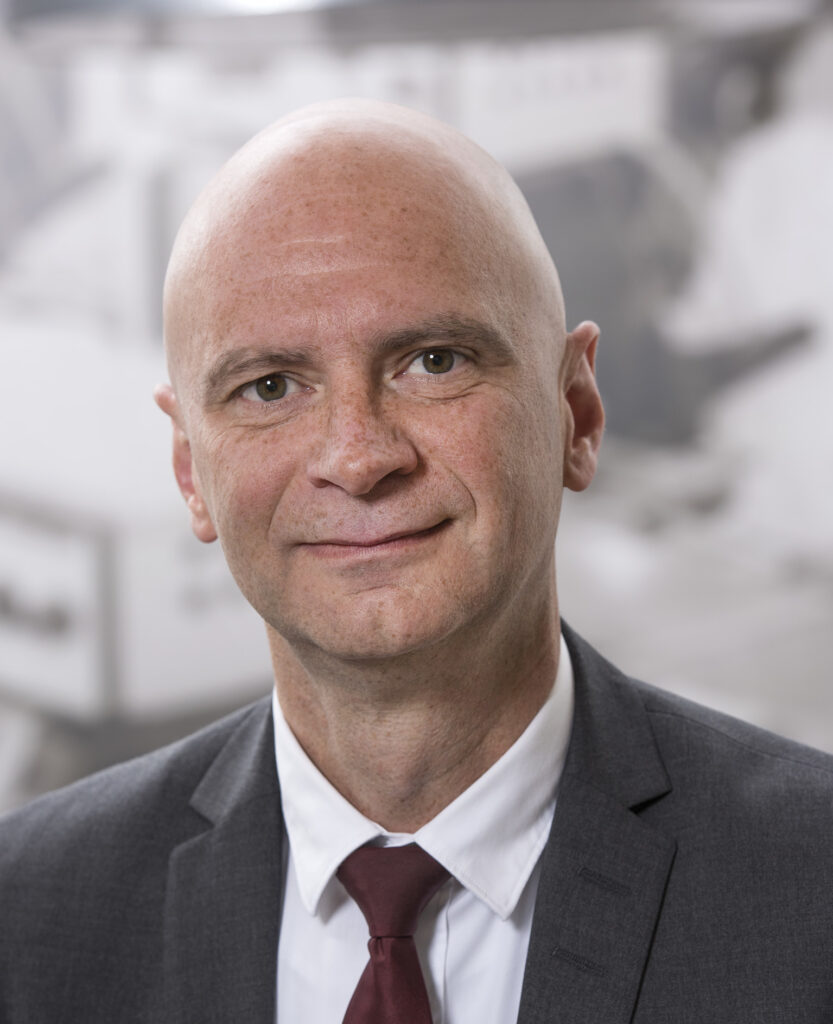
Oliver Maiwald
CEO, Sencio
After developing DECT hardware and software applications at Höft & Wessel, Oliver began his semiconductor career at National Semiconductor as a product application engineer. Here he gained both technical and customer expertise, working on everything from RF and software to full applications. He then went into product marketing at Dialog Semiconductor, where he led efforts to integrate DECT into internet access devices, invented DECT ULE and took part in DECT standardizations at ETSI. In March, 2014 Oliver took over the lead of Sencio B.V.. Oliver holds a master degree in telecommunication engineering from the University of Hannover in Germany.
Abstract:
Flexible wafer back-end processes, that are suitable for low volume and high mix production will be presented using typical examples. In particular, the necessary process steps and possibilities for a Wafer Level Chip Scale Package (WLCSP) from design to implementation will be highlighted. This includes redistribution layer (RDL), under bump metallisation (UBM), wafer thinning (grinding), laser marking, wafer level solder ball attach (Bumping), solder reflow, flux cleaning, wafer mounting and dicing, testing and tape and reel packaging. Results like bump adhesion results by solder shear tests will be shown.
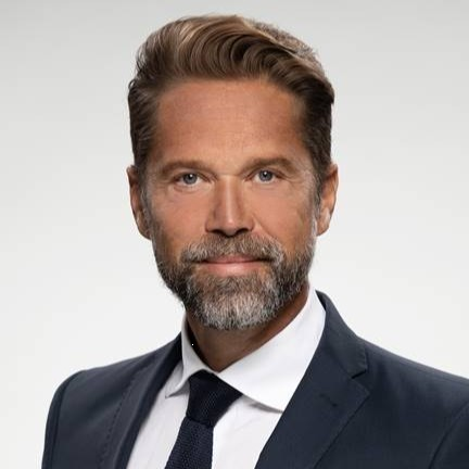
Christian Roessle
Managing Director & President Sales Marketing, MST Group
Christian Rössle has been President of Sales & Marketing at MST for over 3 years, where he orchestrates growth for Class 3 component solutions to improve human health and safety. Previously, Christian Roessle was VP of Sales & Marketing during his 11-year tenure at PCB manufacturer Schweizer Electronic, where he also led partner management for Asian supply chain partners. During his 14-year tenure at Infineon, Christian Roessle held various sales and marketing roles ranging from semiconductors for mobile and consumer memory to power semiconductors for automotive and industrial applications. With a background in industrial engineering and more than 28 years of experience in the microelectronics market, he is passionate about finding interconnect solutions that maximize value for the customer.
Abstract:
This talk highlights the potential of System in Package (SiP) solutions on both organic and ceramic substrates, with a specific emphasis on their production within Europe. Exploring opportunities for domestic manufacturing, the presentation examines how these advanced solutions can thrive in the European market while maintaining competitive advantages.
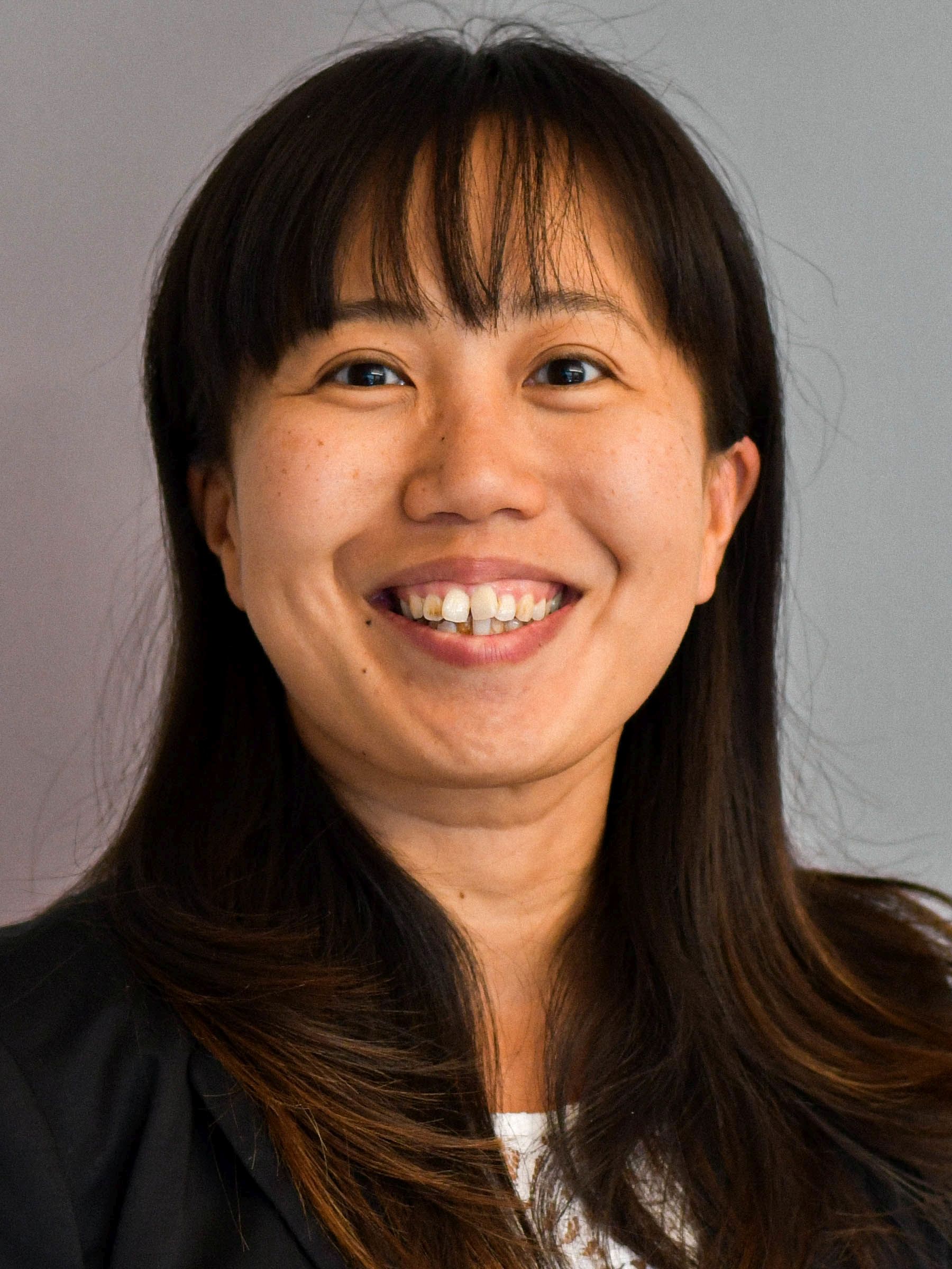
Sy Jiun Sim
Technical Marketing Manager, PacTech
Syjiun Sim joined PacTech in year 2010 during the establishment of its subcontracting site in Penang, Malasyia. With her background in marketing and operations, Miss Sim was focusing on customer support and project management, contributing essentially to the growth of PacTech Asia into the largest subcontracting site of the PacTech Group. Since year 2017, she is located at PacTech’s headquarters in Nauen, Germany, where she is leading the Technical Marketing team on a global scale. Her main responsibilities are identifying potential future markets and shaping of PacTech’s technology roadmap.
Antonio Barny
Grants Senior Manager, Amkor Technology Portugal (ATEP)
Antonio Barny is Grants Senior Manager and joined Amkor in July 2017 as part of the NANIUM acquisition. He started his career at Texas Instruments as Wire Bond engineer and held management positions in Quality and Operations at Siemens and Infineon. Antonio has 10+ years’ experience in Business Development and Sales, and he holds a degree in Electronics Engineering and a Master in Innovation and Technological Entrepreneurship by Porto University.
Abstract:
Amkor Technology, Inc., a leading provider of semiconductor packaging and test services, is the only High-volume Tier 1 OSAT in Europe. Amkor’s facility in Porto, Portugal, is set to be part of EU ecosystem by ensuring supply chain stability, scale and delivering the next-generation semiconductor packaging and test solutions for critical European and Global markets such as automotive, security and industrial.
Bruno Giorgi
VP Worldwide Sales & Marketing, PRESTO Engineering Group
Bruno has more than 25+ years of experience in managing Sales & Marketing in the Electronics & High-tech industries, including 10 years in Executive Management in Semicon. Prior to joining Presto Engineering Group as VP Worldwide Sales & Marketing, Bruno held a number of sales and marketing leadership positions in the connector industry, and Semicon OSAT packaging industry (JCET Group/STATS ChipPAC). Throughout his career in fine micromechanics, fine assemblies and Semicon, he has excelled in developing strong relationships with strategic large-scale customers, and in empowering strong growth sales roadmaps. Bruno received a Master of Science in mechanical engineering from ENSAM Arts & Métiers, and a Master of Advanced Studies in Advanced Industrialisation from ENS Cachan and ENSAM Arts & Métiers, France. He also received High Performance Leadership (HPL) Executive certification from the International Institute for Management Development (IMD) in Lausanne, Switzerland, and Executive Sales practices certification with Sandler, Lausanne, Switzerland.
Abstract:
Analog mixed signal ASIC innovation calls for package and assembly specialty. With the fast growth of sensor technologies requirements, following packaging standards might not be sufficient enough to get device to proper performance. ASIC and Package co-design undergo essential side by side to guarantee manufacturability and reliability. Nevertheless this necessary integration will continue to challenge the device testability advocating for a holistic approach of product design.

Jan de Koning Gans
Managing Director Sales & Marketing
Jan de Koning Gans is Managing Director at RoodMicrotec GmbH and responsible for the companies’ sales and marketing organisation and activities. Prior to joining the company in 2017, he served in sales and management roles at various companies in the semiconductor assembly and test industry, as well as in other, non-semiconductor, markets. After having worked as a computer engineer, Jan entered the semiconductor test business in the late 80’s working for Rood Testhouse in the Netherlands. He gained in-depth experience in the semiconductor assembly and test services business, while working as European sales director for respectively Hyundai Electronics Industries, ChipPAC and STATSChipPAC. Further to his education in electronics engineering, Jan holds a bachelor degree in marketing.
Abstract:
Although not representing the largest share of the global semiconductor market, Europe does house various leading companies supplying advanced semiconductor products to the automotive industry, as well as providing innovative semiconductor solutions for medical, industrial and high-end consumer applications. Among those companies are many ‘fabless’ manufacturers, ranking from well established design & supply companies to innovation-driven start-ups. What all have in common is the dependency on partners, both in front-end, as well as in back-end manufacturing. Time-to-market and first-time-right are of the essence for the company’s success. European based partners can be of great added value in developing, qualifying and launching new products faster, at lower risk.
Daniel Lieske
Senior Expert Advanced Packaging, AEMtec GmbH
Daniel Lieske supports product development and production teams and advises the sales team for new customer projects and technology development. He holds a diploma in microelectronics and microsystems from the Brandenburg University of Technology in Cottbus. Daniel worked as process engineer for Infineon Dresden and Qimonda in the Backend for development, production and process transfer to volume sites of Multi-Chip Modules (MCM). As process engineer at AEMtec he was responsible over the last 12 years for wafer level solder ball attach, printing technologies, solder reflow and failure analysis.
Abstract:
Flexible wafer back-end processes, that are suitable for low volume and high mix production will be presented using typical examples. In particular, the necessary process steps and possibilities for a Wafer Level Chip Scale Package (WLCSP) from design to implementation will be highlighted. This includes redistribution layer (RDL), under bump metallisation (UBM), wafer thinning (grinding), laser marking, wafer level solder ball attach (Bumping), solder reflow, flux cleaning, wafer mounting and dicing, testing and tape and reel packaging. Results like bump adhesion results by solder shear tests will be shown.

Marco Del Sarto
MEMS package design and integration manager, ST Microelectronics Italy
Ing. Marco Del Sarto got his MD in July 2000 in university of Pisa with a work of thesis on Bio-Chip developed in STMicroelectronics. Since 2001 he joined STMicroelectronics as designer for MEMS structure in the field of testing, modelling and simulation. From 2003 to 2006 leaded the technical program manager activities to industrialize first MEMS accelerometer. He covered various roles on quality department on MEMS product from 2006 to 2016 from customer quality assurance to department management. In parallel he leaded the validation and characterization team working on MEMS sensor. Since 2016 he is driving the package design R&D team on MEMS sensors spreading from Motion MEMS, microphone, Pressure sensor and advanced architecture for actuators and IoT sensor nodes.
Abstract:
– How to extend the definition of a 3D package from a pure interconnection point of view to the needs on Sensor world
– Definition of 3rd dimension on sensor: “the sensing path”
– Description of few examples
Rajesh Mandamparambil
Director Path Finding, Package Innovation, NXP Semiconductors
Rajesh has more than 18 years of experience in technology developments in printed, flexible, stretchable, 2.5/3D and main stream semiconductor packaging. He holds a PhD degree in Optoelectronics and has published in more than 100 peer-reviewed journals and has 15 patents. He is currently leading innovations in advanced packaging within Package Innovation organisation at NXP.
Abstract:
The talk will introduce NXPs product focus and drivers in semiconductor packages towards addressing those challenges.

Jeroen Didden
Senior Development Engineering Project Manager, Melexis
– Jeroen Didden obtained a Master in Bioscience engineering at KU Leuven in 2013.
– He obtained his PhD degree (Nanoscale engineering of CO2-selective gas separation membranes) at the same faculty.
– Since 2018 he works for Melexis as Development Engineer focusing on assembly development from prototyping towards high volume production of sensor products
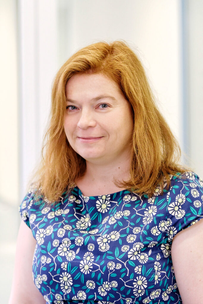
Tanja Braun
Group Manager, Fraunhofer IZM
Tanja Braun studied mechanical engineering at Technical University of Berlin with a focus on polymers and micro systems and joined Fraunhofer IZM in 1999. In 2013 she received her Dr. degree from the Technical University of Berlin. Tanja Braun is head of the group Assembly & Encapsulation Technologies. Recent research is focused on fan-out wafer and panel level packaging technologies and Tanja Braun was leading the Fan-out Panel Level Packaging Consortia at Fraunhofer IZM Berlin. In 2014 she received the Fraunhofer IZM research award and in 2021 the Exceptional Technical Achievement Award from IEEE Electronics Packaging Society (EPS) and the IMAPS Sidney J. Stein Award.

Mark Gortemaker
Sales and Business Development Bruco IC and Manager Bruco Components
Mark Gortemaker (1971) is Sales & Business Development Manager of Bruco Integrated Circuits since January 1st, 2019. Mark started his career at Philips / NXP Semiconductors where he held various positions in quality, reliability, package development, account and customer relation management. From 2007 until 2018 he managed the sales of MASER Engineering parallel to managing the reliability department for 4 years. From April 1st, 2019 onwards Mark also manages the Bruco ASIC supply chain.
Abstract:
Bruco IC is an ASIC design house. Especially ASICS involve low volumes and need a good supply chain. Together with our partners we serve our customers and need a solid European supply chain in silicon, test, but surely in packaging.

Paul van Ulsen
CEO and Owner, Salland Engineering
Paul has over 37 years’ experience in Semiconductor Test and is currently responsible for all aspects of corporate governance and business development for Salland Engineering worldwide. In 1986, Paul started his career as Test Application engineer at Rood Testhouse, where he was involved in many Mixed Signal test solutions. In 1992, he continued as Application engineer at Salland and moved soon into new roles like; project management, HR and Sales which made him decide to choose to be the Sales Director, followed becoming the CEO and in 2017 the owner of Salland Engineering world-wide. In 2018 he acquired Applicos, a leading Analog post-silicon-validation test solution provider, and successfully integrated this into Salland family. In meantime he guided Salland, together with his team, being a worldwide leading and respected player & partner of all top ATE manufactures and being a very advanced and fast(est) growing Engineering & Production Testhouse. He is a graduate of Windesheim Technical University in electronics and computer engineering.
Absract:
This paper is about Salland’s vision about why we believe in a “European semiconductor supply chain, for Silicon validation, Assembly, Wafer & Final testing” that can and needs to exist. It will talk more about how (High Volume) Test solutions comes together, challenges we face on the road towards it, how we dealt with it and show some examples of how we kept the supply chain in The Netherlands with innovative solutions & cooperation.

Gabriela Pereira
Technology & Market Analyst – Advanced Packaging, Yole Développement
– Gabriela Pereira is in the packaging team within the Semiconductor, Memory and Computing Division at Yole Intelligence (Yole).
– She focuses on advanced packaging platforms, develops technology and market reports and is engaged in creating dedicated custom projects.
– Gabriela’s experience in the semiconductor field includes working at Amkor Technology, first for her master’s thesis and then as a R&D Engineer, where she collaborated on several package development projects.
– She holds a master’s degree in Metallurgical and Materials Engineering from the University of Porto, Portugal.
Abstract:
The presentation will share the latest metrics of the Advanced Packaging market including the newest manufacturing capabilities being put in place worldwide with a focus on Europe. European governments are investing in chip manufacturing to strengthen its local supply chain; however, assembly and test capacity is needed to boost time-to-market and decrease overseas dependency. With a 9.1% growth expected for the next five years, advanced packaging has become a critical and effective strategy for improved performance, following the industry’s latest megatrends of AI, HPC and vehicle electrification.

Jan Vardaman
President, TechSearch International
E. Jan Vardaman is president and founder of TechSearch International, Inc., which has provided market research and technology trend analysis in semiconductor packaging since 1987. She is the author of numerous publications on emerging trends in semiconductor packaging and assembly. She served on the NSF-sponsored World Technology Evaluation Center (WTEC) study team involved in investigating electronics manufacturing in Asia. She is a senior member of IEEE EPS and is an IEEE EPS Distinguished Lecturer. She received the IMAPS GBC Partnership award in 2012, the Daniel C. Hughes, Jr. Memorial Award in 2018, the Sidney J. Stein International Award in 2019, and she is an IMAPS Fellow. She is a member of MEPTEC, SMTA, and SEMI. Before founding TechSearch International, she served on the corporate staff of Microelectronics and Computer Technology Corporation (MCC), the electronics industry’s first pre-competitive research consortium.
Abstract:
Regions around the world are preparing to boost domestic capability in semiconductor production, yet substrate production and much of the assembly remains in Asia. Does it solve supply chain concerns if semiconductors are fabricated in Europe, but sent back to Asia for packaging? European companies lead in automotive electronics, MEMS, and power devices. Is this enough? This presentation highlights the strengths of European organizations, the status of high-density substrate production, and assembly capabilities in Europe.Challenges in building a European ecosystem are highlighted.

Eric Fribourg-Blanc
Programme Officer, KDT Joint Undertaking, European Commission
Programme Officer at Key Digital Technologies JU, focusing on research funding related to semiconductor technologies and heterogeneous integration. I have worked for 11 years at CEA-LETI at various positions, including at the laboratory for heterogenous integration, and 4 years as Policy Officer at the European Commission in DG CONNECT. My passion is to bridge the gap between research, technology and industry, to accelerate the transfer of advances made in digital technologies to society. I’m always looking for new opportunities to support the European electronics components and systems players.
Abstract:
The presentation will cover the portfolio of projects supported since the beginning of ECSEL. It will notably show a clear but scattered support to heterogeneous integration and packaging. Further, what is known of the upcoming implementation of the Chips Act will be presented with highlights of important prospects for the packaging community in Europe.
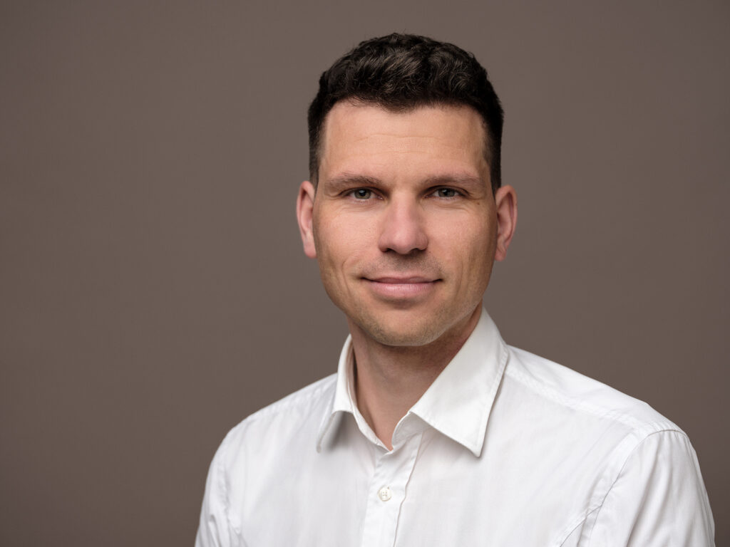
Michael Dittrich
IC Package Design Engineer, Racyics
- Diploma in Information Technology at Technical University of Dresden, Germany, in 2010.
- 1 year in electronic industry
- Joined Fraunhofer IIS (Institute of Integrated Circuits) in 2012
- Work on design and layout of innovative advanced packaging technologies
- In 2020 he joined Racyics and currently is leading the team for IC packaging.
- Ensuring successful integration of customers ICs in state-of-the-art packages.
Abstract:
Racyics is Europe’s leading design house for mixed-signal System-on-Chip design in advanced nodes. Racyics has established a package co-design team to ensure the seamless integration of their ICs in State-of-the-Art IC-packages. During the presentation, we will clarify our understanding of IC-package co-design and highlight why it’s crucial to think about IC-package design from the very beginning of chip development.
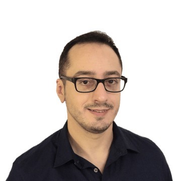
Ayad Ghannam
CEO and Founder, 3DiS Technologies
Ayad Ghannam received Ph.D degree in Microwave, Electromagnetism and Optoelectronic from University of Toulouse III, France, in 2010. During Ph.D, he worked as a research engineer at Freescale Semiconductors, France branch, and LAAS-CNRS where he designed high-Q power inductors and developed an Above-IC process for their integration. After graduation, he continued working in LAAS-CNRS as a research engineer where he developed an innovative 3D interconnect technology. He has more than 20 publications in journals and conferences and 8 patents. He founded 3DiS Technologies in 2014, a spinoff that offers innovating 3D system packaging and 3D IPD solutions based on a novel 3D RDL technology.
Abstract:
For current 4G communication modules, RF components are housed in an RF front-end module, which manages signal amplification and filters noise. The antenna, used for transmitting and receiving radio signals, is separate and not integrated into the module. The major change occurs in 5G/6G modules operating at mmWave frequencies where packages need to be very compact, low loss and integrate antennas inside. 3DiS is developing the next generation of advanced 3D packaging solutions for RF applications, integrated at the wafer level (3D-WLP), using its 3D-RDL technology, which features low-loss RF transitions and antennas in-package (AiP). Their proprietary technology of dielectric core Through Package Vias (HDc-TPV) allows for high-aspect-ratio, highly conformal vertical interconnections that are formed simultaneously with the 3D-RDL layer. 3DiS will showcase its latest technological advancements for wafer-level system packaging, as well as the implementation of these technologies, particularly in the context of Chip-Package-Board design.
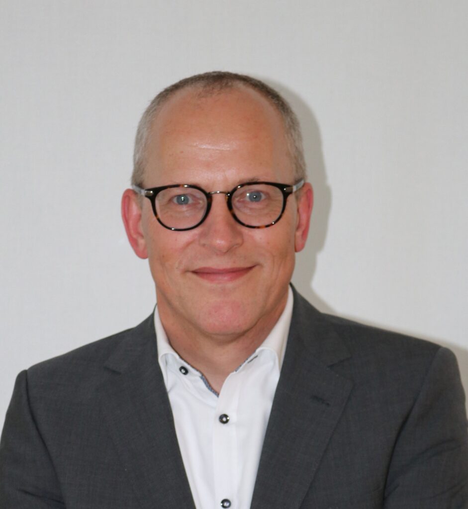
Ruud de Wit
Business Development Manager, Henkel Electronic Materials
Ruud de Wit is responsible for managing Henkel’s Semiconductor, Sensor & Consumer Electronics Assembly Materials’ business development within EMEA. Ruud has a BSc degree in Mechanical Engineering followed by several polymer, sales, and marketing courses. Ruud is working for Henkel since 1990 in multiple positions, including technical customer support, quality assurance and engineering, and global semiconductor account and product management. Last couple of years, Ruud’s focus is on exploring and driving new and advanced semiconductor packaging material development needs within Henkel, with emphasis on Wafer Level Packaging and Pressure-less Silver Sintering die attach on Cu lead frames.
Abstract:
This 15min ‘high-speed’ presentation prepared for this EuroPAT workshop will cover the latest innovations in semiconductor liquid encapsulation materials used for Fan-Out Wafer-Level molding and printing processes, alongside new developments in advanced liquid underfills for larger chip sizes enabling next generation 2.5/3D package designs.
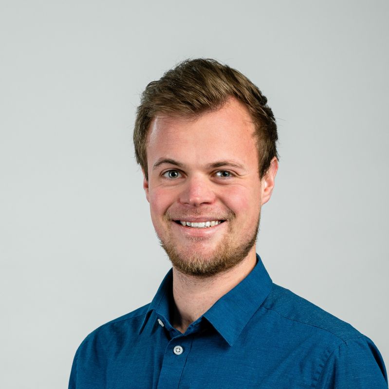
Jan-Philipp Wessels
Application Engineer, Lidrotec GmbH
– Since Jan 2023: Application Engineer at Lidrotec
– 2021-2022: Scientific Assistant at Laserzentrum Fachhochschule Münster with responsibility for ultrashort pulsed laser Micromachining
– Studies in Laser Technology at FH Münster, RWTH Aachen and Fraunhofer ILT
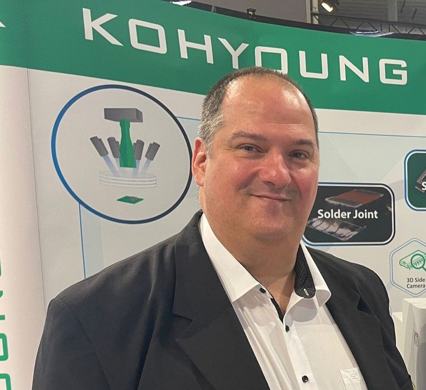
Michael Zahn
Sales Manager, Koh Young Europe GmbH
After completing his technical vocational training, Michael Zahn pursued part-time Bachelor Professional and Master Professional studies in Production Technology and MBA while simultaneously beginning his career in the electronics industry in 1994. He commenced his journey in 1994 by building electrical and optical inspection systems for Bare PCBs and inner layers at Mania Technologie AG. In 2001, he transitioned to DEK Printing Machines, assuming various management positions within Germany, Europe, and globally. During his tenure with DEK, Michael filed and obtained several patents, showcasing his extensive technical knowledge. Due to his profound expertise, he was appointed as the Business Manager for the Singapore subsidiary, relocating there with his family. In this role, he primarily focused on Semiconductor Manufacturing processes and Back-end assembly solutions. After spending four years in Asia, he returned to Germany in 2016 and assumed the position of Global Business Development Manager at Christian Koenen GmbH, a leading company in Tools for the Printing Technology sector, with a specific emphasis on the Semiconductor Industry and emerging markets. In March 2023, Michael has once again ventured into the Inspection Systems Industry. He joined Koh Young Europe GmbH as a Sales Manager, with a special focus on the Semiconductor Industry.
Abstract:
The last years were shaped by new innovations in consumer and communication industry. Wearable electronics were getting smaller versus an increased functionality and data transfer rate. On the production side we saw this trend as well: smaller components, higher density, more functionalities, high frequencies. At the end, we got blurring boundaries between front-end, backend and, second assembly (SMT). From the equipment side we see this trend as well, but there are still harsh requirements and challenges in the semiconductor packaging. The presentation will show solutions to integrate state of the art SMT measurement technology into semiconductor packaging applications.
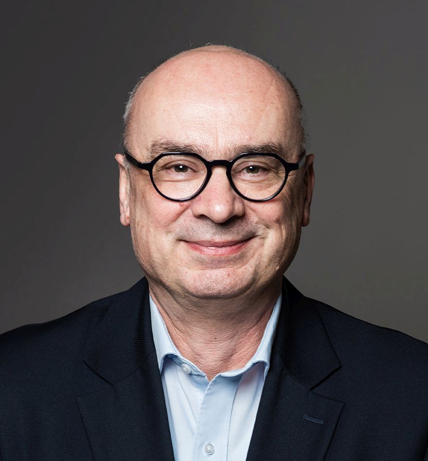
Michael Arnold
Managing Director, PEER Group GmbH
- Graduation from Friedrich-Schiller University Jena in 1986 with a Diploma degree in Physics.
- In 1994 Ph.D in Physics.
- Work and industry experience:
- R&D projects in optical thin film technologies with Zeiss
- Missile development program in German defense industry
- Application of factory automation solutions in various industries at Matsushita
- Since 2001 different management roles in semiconductor industry
Abstract:
Factory automation in semiconductor front manufacturing is based on SEMI standards. The implementation of the related SEMI standards significantly contributed to the productivity improvements in fabs. Labor shortage, supply chain requirements, and the need for further productivity improvements drive digitalization in back end manufacturing. Adopting and implementing SEMI standards will help to overcome current constrains in backend manufacturing that limit productivity.
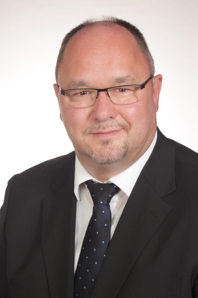
Steffen Kröhnert
President & Founder ESPAT-Consulting
- Before starting ESPAT-Consulting in June 2019, worked for 22 years in different Semiconductor Packaging R&D, Engineering, and Management positions at large IDMs and OSATs in Germany and Portugal (Siemens, Infineon, Qimonda, NANIUM, and Amkor)
- In 2016 founded and since chaired or co-chaired the European SEMI-integrated Packaging, Assembly, and Test – Technology Community (ESiPAT-TC), a special interest group focusing on manufacturing in Europe
- Authored or co-authored 23 patent filings and many technical papers in the field of Packaging Technology, and co-edited two textbooks about “Embedded and Fan-Out Wafer and Panel Level Packaging Technologies”
- Active member of many technical and conference committees of IEEE EPS, SEMI, IMAPS, and EPoSS.
- Holds an M.Sc. in Electrical Engineering and Microsystems Technologies from the Technical University of Chemnitz, Germany.

Edsger Smits
Program Manager CITC
- PhD in thin film electronics from the University of Groningen with a focus on flexible transistors.
- 10 years of experience as researcher and program manager in flexible and stretchable electronics at Holst Centre.
- For 2 years program manager at CITC leading the thermal high-performance packaging program.
